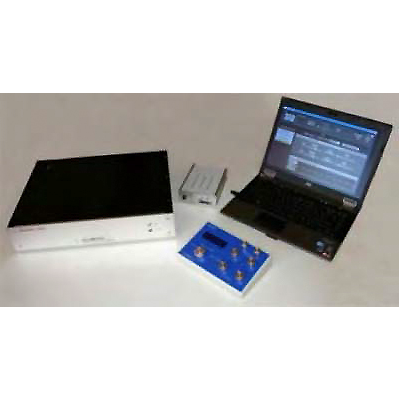
Materials science properties (metals, alloys, ceramics, semiconductors, nanoparticles) depend on great extent on their textures at nm scale level. ASTAR device uses TEM based orientation mapping technique (EBSD-TEM like) based on collection of precession electron diffraction (PED) patterns and cross-correlation comparison with simulated intensities.
ASTAR can turn any TEM into a very powerful analytical tool enabling orientation–phase imaging at 1 nm resolution attainable (FEG TEM) in combination with other TEM analytical techniques.